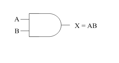
The gate which is used for logical multiplication is called AND logic gate. It is a basic digital logic gate. This gate can have two or more inputs but the output will be one. In this case, if the input is A and B then the output will be Y = AB. The output of AND gate will be equal to the logical product of the inputs.
The logic diagram of AND gate is as follows:
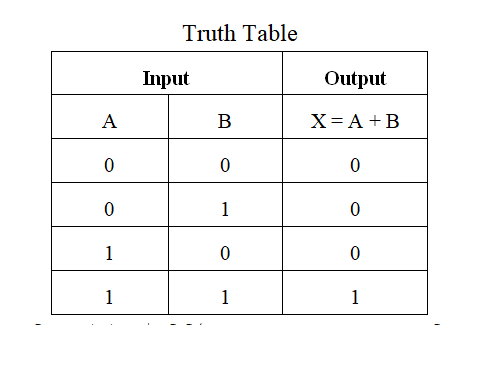
The truth table of AND Logic Gate is given below:
Here, if all the inputs are 1, only the output is 1, otherwise, the output will be 0.
Circuit diagram of AND gate
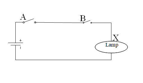
The figure shows a circuit consisting of a series of ways co-equivalent to the AND gate. If you switch on any one of the two switches in this circuit, the lamp will not light up. The lamp will only light when two switches are on.
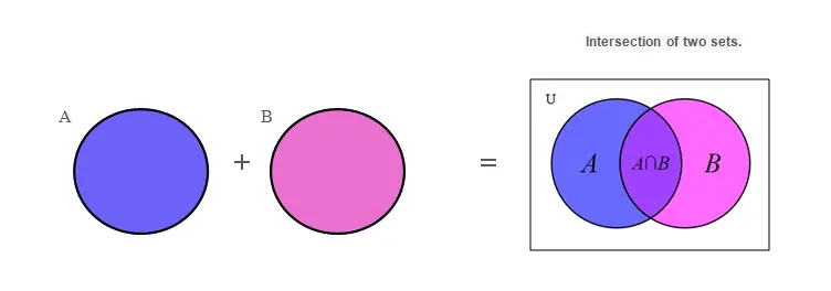
AND gate using set theory:
We can also explain AND function using set theory. Suppose, two sets A and B together form U universal set. The universal set shows the structure of the AND gate in the Venn diagram.
Transistor Circuit Diagram of AND Gate
We can also explain AND logic gate using the transistor AND gate. The circuit diagram of a transistor AND gate is given below:
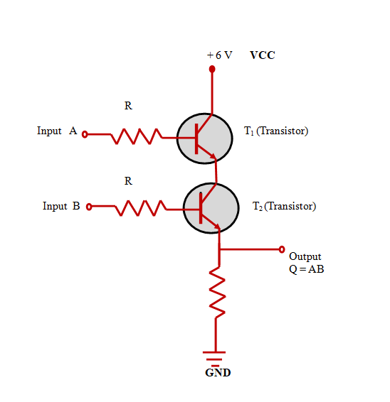
Here the circuit shows both the inputs A & B for the AND gate and output Q. The inputs A & B are joined to the base terminal of two NPN Transistor T1 and T 2, respectively that control the supply of electricity. The output Q is connected to the LED (Light Emitting Diode) that displays the status of output. When both A and B are at o V potential at transistor T1 or T2 and both, T1 and T2 will be in OFF conditioned respectively and the output LED will be OFF. If there is a voltage supply at both the transistors the inputs will be 1 and the output LED will be glow.
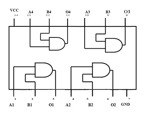
AND Gate IC 7408
7408 IC is a QUAD 2-Input AND GATES. 7408 IC contains four independent gates each of which performs the logic AND function. Four AND gate is in 14 Pin DIP IC.
Related term :
